Another PWM controls a switching voltage regulator
A PWM-controlled regulator, this time using a logic gate IC, op-amp, and resistors and capacitors to buffer the PWM signal. The post Another PWM controls a switching voltage regulator appeared first on EDN.

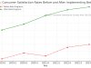
A recent Design Idea, “Three discretes suffice to interface PWM to switching regulators,” demonstrated one way to use PWM to control the output of a typical switching voltage regulator. There were some discussions in the comments section about circuit behavior, which influenced design modification. Here’s a low-cost design that evolved in light of those discussions. A logic gate IC, an op-amp, and a few resistors and capacitors buffer a PWM and supplies a signal to the regulator’s feedback pin, Figure 1.

Figure 1 A microprocessor produces a 12-bit, 20 MHz, PWM signal that controls a switching voltage regulator using an inverter IC, an op-amp, resistors, and capacitors to buffer the signal for the regulator’s feedback pin.
Wow the engineering world with your unique design: Design Ideas Submission Guide
For various reasons, it’s difficult, if not impossible, to control a regulator’s output voltage beyond a certain level of accuracy. This design proceeds with a PWM having 12 bits of resolution in mind, operating at a frequency of approximately 4900 Hz.
It’s easy these days to find microprocessors (µPs) that can produce a PWM clocked at 20 MHz. However, the supply currents running through that IC’s power supply bonding wires can cause voltage drops. This means that the PWM signals don’t quite swing to the rails. Worse yet, if the currents vary significantly with the µP’s tasks, the voltage drops can change, and it might not be possible to calibrate the errors out. A simple solution is to buffer the µP with logic gates (typically inverters), which draw negligible current except during switching transients. The gates can be powered from a clean, accurate voltage source, the same as or close in value to that which powers the µP.
The inverter in Figure 1 is a 74LVC2G14GW,125 IC whose paralleled outputs drive an op-amp-based low-pass filter whose passive components are of sufficiently high impedances to negligibly load those outputs. When powered from 3 V or more, this dual inverter has an output resistance of less than 15 Ω from -40°C to +85°C. (If you need to operate the µP at 1.8 V, parallel the 6 inverters of a 74LVC14AD,118 for a less than 19 Ω result.)
The TLV333IDBVR op-amp has a maximum input offset voltage of 15 µV (the maximum offset is specified for a 5-V supply; an unknown increase can be expected if the supply voltage is lower).
Its typical (maximum are not specified) input currents are 150 pA from -40°C to +85°C, contributing an offset through R1, R2, and R3 of 115 µV. At 1.8 V, ½ LSb for a 12-bit signal is 220 µV (370 µV with a 3.0-V supply.) The filter settles to much less than that 12-bit ½ LSb voltage in 10mS and has a peak (not peak-peak) ripple of less than 50µV.
R4 and R5 should be chosen so that the intended most positive op-amp output voltage multiplied by R4 / (R4 + R5) is at most slightly greater than Vfb. This allows a regulator output of Vfb. This ratio could be smaller if the minimum desired regulator output is larger than Vfb. The resistors’ parallel combination should be the value specified by the regulator for the single resistor connected between Vfb and ground, typically 10 kΩ. R6 should be set in accordance with the desired range of output voltages.
The allowed range of PWM duty cycles should exclude extremes for at least two reasons. First, the op-amp output is only guaranteed to swing within 70 mV of each rail (with a 10k load connected to half of the supply voltage.) Second, the processor, GPIO in particular (but also the gate to some extent), likely has unequal rise and fall times and delays. Although these differences are small, they have their greatest effects on accuracy at duty cycle extremes, which therefore should be avoided. Fortunately, accommodating these limitations has a negligible effect on functionality.
In this design, the output voltage is linear with the duty cycle. The regulator’s loop gain is unchanged from that of standard operation. With the regulator disabled until the PWM filter output settles, there are no startup issues. Finally, there is negligible inherent injection of noise into the feedback pin from an external supply.
Christopher Paul has worked in various engineering positions in the communications industry for over 40 years.
Related Content
- Three discretes suffice to interface PWM to switching regulators
- Control an LM317T with a PWM signal
- PWM power DAC incorporates an LM317
- Tracking preregulator boosts efficiency of PWM power DAC
- 1-A, 20-V, PWM-controlled current source
- Clearing out the data clutter
The post Another PWM controls a switching voltage regulator appeared first on EDN.
What's Your Reaction?